 |
Search | FAQ | US Titles | UK Titles | Memories | VaporWare | Digest | |||||||
| GuestBook | Classified | Chat | Products | Featured | Technical | Museum | ||||||||
| Downloads | Production | Fanfares | Music | Misc | Related | Contact | ||||||||
| CED in the History of Media Technology | ||||||||||||||

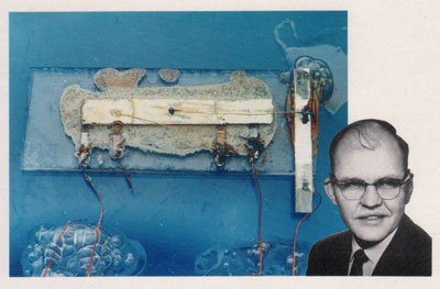
After the invention of the transistor a practice emerged where components were connected together by mounting them on ceramic wafers that could be stacked one atop the other into assemblies called micromodules. This concept saved space, but didn't reduce the number of connections needed. Jack Kilby, an engineer at Texas Instruments, envisioned eliminating the connections by selectively doping the surface of silicon so various regions on a monolithic piece of the material could function as transistors, diodes, resistors, and capacitors. Kilby completed his first device (pictured) on September 12, 1958 which was actually constructed on germanium rather than silicon, as he could not find a suitable piece of silicon at the time. But the integrated circuit was fully functional, and TI officially announced it in January 1959.